In an ideal metal, the bonding molecular orbitals extend over the whole sample. For simplicity, we just consider a long chain of atoms, i.e. an one-dimensional metal where each atom has one single valence electron in an s-orbital. The linear combination of atomic orbitals are obtained by linearily stringing together all atoms. Then, we determine the electronic configuration in accordance with the building-up principle.
Band Structure
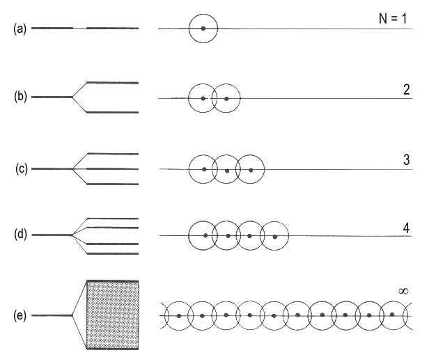 |
| Fig. 1: The formation of a band of N orbitals as a result of adding single atoms to a chain. The band keeps a certain width and, in practice, features a continuum of energy levels though it consists of N discrete orbitals. |
A single atom has an s-orbital of a certain energy (Fig. 1a). If a second atom is added, one bonding and one antibonding molecular orbitals will be formed (Fig. 1b). The third atom overlaps with the neighbouring and, to some extent, the next but one atom. Three molecular orbitals are obtained (Fig. 1c). Adding a fourth atom yields a fourth orbital (Fig. 1d). The effects of adding further atoms are obvious. The number of orbitals grows and the range of energies of the molecular orbitals is extended. Assuming a chain of N atoms, a band of N molecular orbitals are found between one minimal and one maximal energy value. In Hückel's description, a secular determinant of the following kind appears:
| |
| | | | | |
x | 1 | 0 | 0 | 0.... | 0 | |
| | | | | |
= 0 |
| 1 | x | 1 | 0 | 0.... | 0 | |||
| 0 | 1 | x | 1 | 0.... | 0 | |||
| : | : | : | : | : | : | |||
| : | : | : | : | : | : | |||
| 0 | 0 | 0 | 0 | 0.... | x |
A general solution to such a determinant is
E = α + 2 β cos{kπ/(N+1)} , k = 1, 2, ..... N
For N approaching infinity, the distance between neighbouring energy levels k and k+1 approaches zero. Nevertheless, the band, i.e. all the resulting orbitals, are confined by the energy values for k = 0 and k = N. For N → ∞, the width of the band is -4β. We imagine this band as being composed of N molecular orbitals of which the lowest (for k = 0) is completely bonding and the highest (for k = N) is completely antibonding.
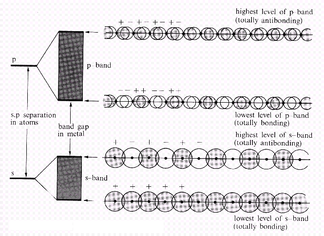 |
| Fig. 2: An overlap of s-orbitals leads to an s-band, an overlap of p-orbitals to an p-band. In the case shown here, the energy difference between s- and p-orbitals prevents both bands from overlapping and a gap remains. In cases with smaller distances between s- and p-orbitals, both bands merge. |
A band resulting from an s-s-overlap is an s-band. For atoms where p-orbitals have to be considered, a p-band will be present as well (Fig. 2). For p atomic orbitals above the s orbitals, the p band will be as well above the s band. Dependent on the involved atoms, the bands are found to be separated by an energy band gap.
 |
|
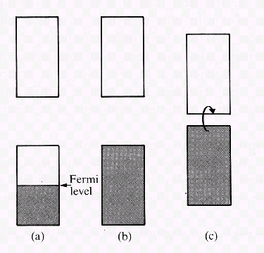
| Fig. 3: In a situation where (a) N electrons occupy a band of N orbitals, the band is half filled and the electrons near the Fermi level remain mobile. (b) With 2N electrons, the band is full and the material is an insulator. (c) If there is a narrow gap between the full band and an empty one above, the material can display semiconductivity. This properity is explained by electrons located in the higher band. Electrons in this state are surplus electrons introduced by doping pure crystals with adequate heteroatoms or electrons excited due to thermal conditions. |
Let us consider a metal where each atom contributes with one electron to the structure of the solid (e.g. alkali metal). We find N molecular orbitals apparently forced into a narrow band. N electrons are present in this band and therefore only ½N orbitals are filled by a pair of electrons. The Fermi level is the uppermost filled orbital. As orbitals of somehow higher energy exist, little energy suffices to transfer electrons into these orbitals. Such excited electrons move easily within the solid, i.e. their occurence explains electric conductivity, a phenomenon present in solids where partially filled bands exist.
Insulators and Semiconductors
If each atom contributes with two electrons, we will find 2 N electrons in N orbitals. The Fermi level is then located at the upper limit of the band (Fig. 3b). A gap separates this band from another band of higher energy. In this situation there are no mobile electrons, thus we observe no electric conductivity and speak of an insulator. Solid helium is an example for such an insulator whereas the elements of the second main group like beryllium form an s- and an p-band that overlap. As a consequence, electrons are able to leave the full s-band and move within the p-band, i.e. beryllium shows conductivity.
There are as well materials where the band gap is quite narrow (Fig. 3c). They are insulators, but provided that some electrons have been excited in a way that they have been transferred in the upper band, electric conductivity is found. Such materials are classified as semiconductors. There are several possibilities for such an excitation. In case the width of the gap is below kT, already temperature T suffices to have mobile charges. The higher temperature T is, the higher is the conductivity of the material. (In contrast, the conductivity of metals decreases with increasing temperature.) As well, controlled addition of certain impurities to highly pure substances may lead to semiconductivity. Such doted atoms can contribute less electrons than a 'regular' atom, in other words, they introduce empty positions within a band. An electron from elsewhere is able to fill such a position. In turn, another position becomes empty. Thus, empty positions appear to be mobile and conductivity (of p-type) is observed. In analogy, the doted atoms may introduce additional electrons (for example phosphorus in a germanium crystal). These electrons are found in a previously empty band and represent mobile negative charges. In consequence, such doted solids are said to show semiconductivity of n-type (for negative).
![]()
Auf diesem Webangebot gilt die Datenschutzerklärung der TU Braunschweig mit Ausnahme der Abschnitte VI, VII und VIII.